
Modern electronics are denser, smaller, and more powerful, pushing printed circuit boards to new limits. HDI and complex multilayer PCBs are critical for devices from smartphones to aerospace systems. Building these advanced boards requires precise coordination between design, manufacturing, and assembly, making turnkey pcb assembly the preferred approach for quality, reliability, and speed.
HDI and Multilayer Challenges
HDI and multilayer designs have technical hurdles: fine trace widths, microvias, and stacked layers require exact control in both fabrication and assembly. Even minor misalignments can compromise signal integrity. Managing these tasks across vendors adds risk, as inconsistencies often emerge between teams.
Why Turnkey Is Ideal
A turnkey assembly approach simplifies the entire process by integrating PCB fabrication, component sourcing, and assembly under one roof. This eliminates coordination errors between different vendors, ensures design-for-manufacturability (DFM) consistency, and accelerates delivery timelines. For engineers working on dense, multilayer builds, turnkey solutions reduce handoff friction, enable faster design iterations, and maintain traceability and accountability throughout production.
Stack-Up and Material Considerations
Complex multilayer boards rely heavily on optimized stack-ups and material choices. Factors like dielectric constant, copper thickness, and thermal expansion rate affect impedance control and long-term reliability. A unified turnkey assembly for complex boards ensures that the same engineering team manages both stack-up definition and material procurement, avoiding mismatches that could impact performance. This collaboration enables faster validation of design parameters and smoother transitions from prototype to production.
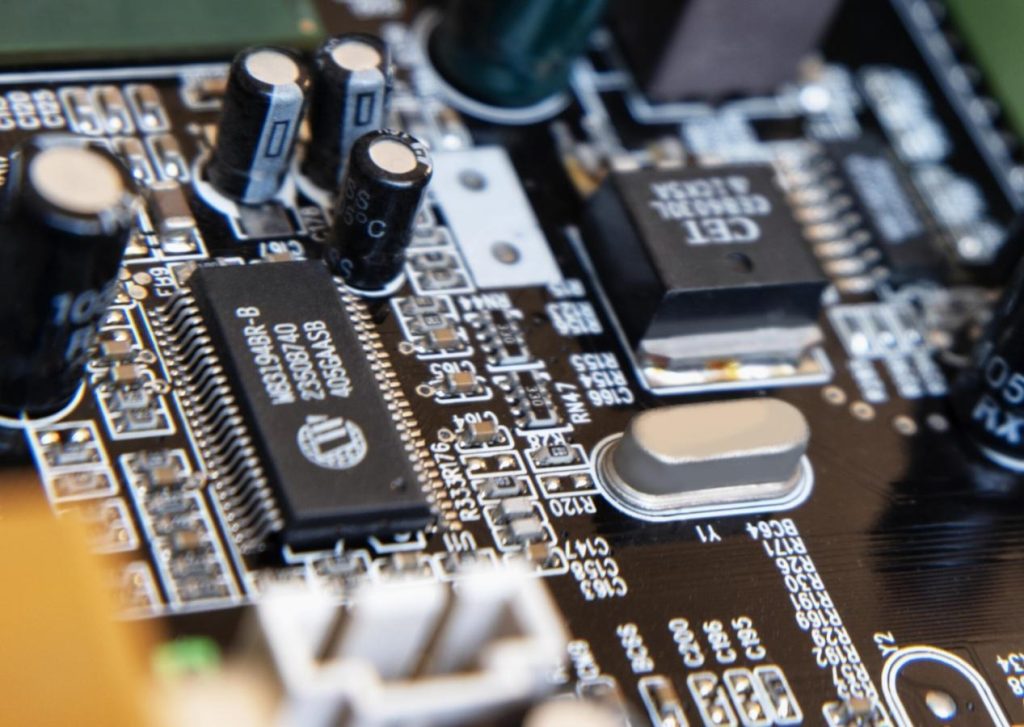
Assembly Complexity and Precision
When dealing with fine-pitch BGAs, 0201 components, or high-layer-count boards, precision assembly becomes critical. Turnkey assembly capabilities include automated pick-and-place, reflow profiling, X-ray inspection, and automated optical inspection (AOI). These processes ensure that solder joints and microvias meet strict IPC standards, maintaining consistency across every batch. Turnkey partners also streamline the process of managing component lifecycle risks and part substitutions—key for high-density projects that can’t afford rework delays.
Quality Assurance and Testing
Comprehensive testing under turnkey workflows includes functional, flying-probe, and ICT testing to verify all interconnections early and avoid rework. Integrated DFM and DFA feedback further boost reliability and manufacturability.
FastTurn PCB Capability Highlights
FastTurn PCB specializes in turnkey PCB assembly for HDI and high-density multilayer designs, offering engineering-driven solutions that minimize production risk. Their advanced in-house capabilities include laser drilling for microvias, multilayer lamination expertise, and precision SMT assembly. FastTurn’s process control and real-time communication platform give engineers visibility from design to delivery—ensuring every build meets performance and quality expectations.
Conclusion
In the world of complex HDI and multilayer PCB design, precision and integration are everything. A turnkey PCB assembly approach provides the alignment, speed, and quality assurance that modern electronics demand. With industry-leading expertise and end-to-end control, FastTurn PCB helps engineering teams bring high-density innovations to market faster and more reliably than ever.